Discontinued On Mar. 2026
VT-S530
PCB Inspection System
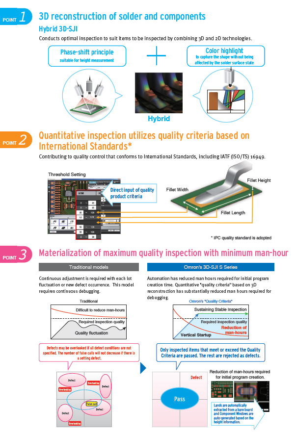
Omron's 3D-SJI (Solder Joint Inspection) Ensuring High-quality Products in an Efficient Manufacturing Environment
* Information in this page is a reference that you created on the basis of information in the product catalog before the end of production, may be different from the current situation, such as goods for / supported standards options / price / features of the product. Before using, please check the compatibility and safety system.
Related Contents
last update: April 15, 2019
Omron's 3D-SJI (Solder Joint Inspection)
Materializes quantitative inspection of solder joint and implementation, while minimizing risks of overlooking unknown defects by the quality product criteria inspection based on the standards, contributing to vertical startup of inspection.
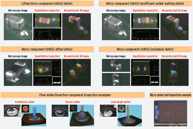
Example Defects
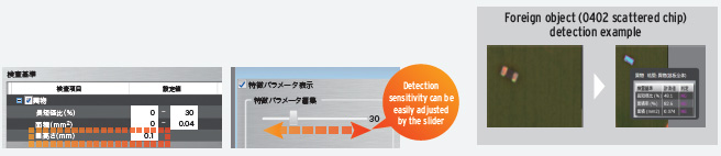
Whole PCB surface inspection
Detecting foreign objects accurately is achieved through combining 3D (height) and 2D (area) measurements on the entire PCB surface. (Lands without solder can be excluded from the inspection)
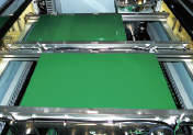
High productivity inspection
High production throughput supported through dual lane.
Dual lane operation using various PCBs is possible, due to its handling capability up to the PCB size of 510 (W) x 330 (D) mm.
last update: April 15, 2019
 Product Category
- Inspection System
-
PCB Inspection System
-
Discontinued
- VT-S530
-
Discontinued
-